Our official English website, www.x-mol.net, welcomes your
feedback! (Note: you will need to create a separate account there.)
Solution-Based Synthesis of Few-Layer WS2 Large Area Continuous Films for Electronic Applications.
Scientific Reports ( IF 3.8 ) Pub Date : 2020-02-03 , DOI: 10.1038/s41598-020-58694-0
Omar A Abbas 1 , Ioannis Zeimpekis 1 , He Wang 2 , Adam H Lewis 1 , Neil P Sessions 1 , Martin Ebert 3 , Nikolaos Aspiotis 1 , Chung-Che Huang 1 , Daniel Hewak 1 , Sakellaris Mailis 1, 4 , Pier Sazio 1
Scientific Reports ( IF 3.8 ) Pub Date : 2020-02-03 , DOI: 10.1038/s41598-020-58694-0
Omar A Abbas 1 , Ioannis Zeimpekis 1 , He Wang 2 , Adam H Lewis 1 , Neil P Sessions 1 , Martin Ebert 3 , Nikolaos Aspiotis 1 , Chung-Che Huang 1 , Daniel Hewak 1 , Sakellaris Mailis 1, 4 , Pier Sazio 1
Affiliation
|
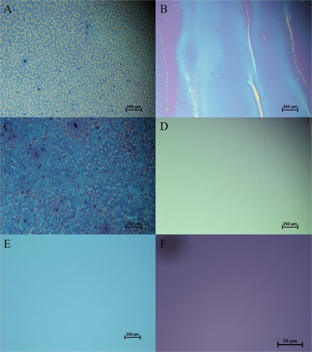
Unlike MoS2 ultra-thin films, where solution-based single source precursor synthesis for electronic applications has been widely studied, growing uniform and large area few-layer WS2 films using this approach has been more challenging. Here, we report a method for growth of few-layer WS2 that results in continuous and uniform films over centimetre scale. The method is based on the thermolysis of spin coated ammonium tetrathiotungstate ((NH4)2WS4) films by two-step high temperature annealing without additional sulphurization. This facile and scalable growth method solves previously encountered film uniformity issues. Atomic force microscopy (AFM) and transmission electron microscopy (TEM) were used to confirm the few-layer nature of WS2 films. Raman and X-Ray photoelectron spectroscopy (XPS) revealed that the synthesized few-layer WS2 films are highly crystalline and stoichiometric. Finally, WS2 films as-deposited on SiO2/Si substrates were used to fabricate a backgated Field Effect Transistor (FET) device for the first time using this precursor to demonstrate the electronic functionality of the material and further validate the method.
中文翻译:

用于电子应用的少层 WS2 大面积连续薄膜的基于溶液的合成。
与 MoS2 超薄膜不同的是,电子应用中基于溶液的单源前驱体合成已被广泛研究,使用这种方法生长均匀且大面积的少层 WS2 薄膜更具挑战性。在这里,我们报告了一种生长少层 WS2 的方法,该方法可产生厘米级连续且均匀的薄膜。该方法基于旋涂四硫代钨酸铵((NH4)2WS4)薄膜的热解,通过两步高温退火,无需额外硫化。这种简便且可扩展的生长方法解决了以前遇到的薄膜均匀性问题。使用原子力显微镜 (AFM) 和透射电子显微镜 (TEM) 来确认 WS2 薄膜的少层性质。拉曼和 X 射线光电子能谱 (XPS) 显示合成的少层 WS2 薄膜具有高度结晶性和化学计量性。最后,首次使用沉积在 SiO2/Si 基板上的 WS2 薄膜来制造背栅场效应晶体管 (FET) 器件,以展示该材料的电子功能并进一步验证该方法。
更新日期:2020-02-03
中文翻译:
用于电子应用的少层 WS2 大面积连续薄膜的基于溶液的合成。
与 MoS2 超薄膜不同的是,电子应用中基于溶液的单源前驱体合成已被广泛研究,使用这种方法生长均匀且大面积的少层 WS2 薄膜更具挑战性。在这里,我们报告了一种生长少层 WS2 的方法,该方法可产生厘米级连续且均匀的薄膜。该方法基于旋涂四硫代钨酸铵((NH4)2WS4)薄膜的热解,通过两步高温退火,无需额外硫化。这种简便且可扩展的生长方法解决了以前遇到的薄膜均匀性问题。使用原子力显微镜 (AFM) 和透射电子显微镜 (TEM) 来确认 WS2 薄膜的少层性质。拉曼和 X 射线光电子能谱 (XPS) 显示合成的少层 WS2 薄膜具有高度结晶性和化学计量性。最后,首次使用沉积在 SiO2/Si 基板上的 WS2 薄膜来制造背栅场效应晶体管 (FET) 器件,以展示该材料的电子功能并进一步验证该方法。


 京公网安备 11010802027423号