当前位置:
X-MOL 学术
›
J. Mater. Chem. C
›
论文详情
Our official English website, www.x-mol.net, welcomes your
feedback! (Note: you will need to create a separate account there.)
Microfluidic solution-processed organic and perovskite nanowires fabricated for field-effect transistors and photodetectors
Journal of Materials Chemistry C ( IF 5.7 ) Pub Date : 2020/01/09 , DOI: 10.1039/c9tc05628a
Ping-An Chen 1, 2, 3, 4, 5 , Jing Guo 1, 2, 3, 4, 5 , Mehdi Nouri 6, 7, 8, 9 , Quanyang Tao 2, 3, 4, 5, 10 , Zhiwei Li 2, 3, 4, 5, 10 , Qianyuan Li 2, 3, 4, 5, 10 , Lulu Du 5, 11, 12, 13, 14 , Huajie Chen 5, 11, 12, 13, 14 , Zaizai Dong 5, 15, 16, 17, 18 , Lingqian Chang 5, 15, 16, 17, 18 , Yuan Liu 2, 3, 4, 5, 10 , Lei Liao 1, 2, 3, 4, 5 , Yuanyuan Hu 1, 2, 3, 4, 5
Affiliation
|
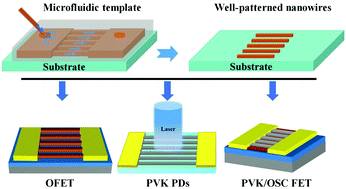
Solution-processed semiconductor nanowires are attractive for application in low-cost and high-performance electronic devices. However, current approaches for nanowire preparation face the problems of having low-throughput and poor controllability of the dimension and location of nanowires. Here we report a simple yet efficient method to implement solution-processable semiconductor nanowires using microfluidics. The method enables fabrication of semiconductor nanowires with high uniformity and well-defined sizes, as well as precise control of their location and alignment in device assembly. Moreover, this method is found to be applicable to various semiconductors, including organic semiconductors (OSCs) and metal-halide perovskites. Furthermore, we have shown the feasibility of employing these semiconductor nanowires to construct different types of devices like field-effect transistors (FETs) and photodetectors (PDs). In particular, lateral heterojunctions consisting of perovskite/OSC nanowires were obtained by this method, based on which high-performance phototransistors were achieved. Overall, the demonstrated method provides a promising route to the fabrication and application of nanowire-based devices.
中文翻译:

微流体溶液处理的有机和钙钛矿纳米线,用于场效应晶体管和光电探测器
溶液处理的半导体纳米线对于低成本和高性能电子设备的应用很有吸引力。然而,当前的纳米线制备方法面临着纳米线的尺寸和位置的低通量和差的可控制性的问题。在这里,我们报告了一种简单而有效的方法,以使用微流体技术来实现可溶液处理的半导体纳米线。该方法使得能够制造具有高均匀性和明确定义的尺寸的半导体纳米线,并且能够精确控制其在装置组装中的位置和对准。而且,发现该方法适用于各种半导体,包括有机半导体(OSC)和金属卤化物钙钛矿。此外,我们已经展示了使用这些半导体纳米线来构造不同类型的器件(如场效应晶体管(FET)和光电探测器(PD))的可行性。特别地,通过该方法获得了由钙钛矿/ OSC纳米线组成的横向异质结,在此基础上获得了高性能的光电晶体管。总体而言,已证明的方法为纳米线基器件的制造和应用提供了一条有希望的途径。
更新日期:2020-02-20
中文翻译:
微流体溶液处理的有机和钙钛矿纳米线,用于场效应晶体管和光电探测器
溶液处理的半导体纳米线对于低成本和高性能电子设备的应用很有吸引力。然而,当前的纳米线制备方法面临着纳米线的尺寸和位置的低通量和差的可控制性的问题。在这里,我们报告了一种简单而有效的方法,以使用微流体技术来实现可溶液处理的半导体纳米线。该方法使得能够制造具有高均匀性和明确定义的尺寸的半导体纳米线,并且能够精确控制其在装置组装中的位置和对准。而且,发现该方法适用于各种半导体,包括有机半导体(OSC)和金属卤化物钙钛矿。此外,我们已经展示了使用这些半导体纳米线来构造不同类型的器件(如场效应晶体管(FET)和光电探测器(PD))的可行性。特别地,通过该方法获得了由钙钛矿/ OSC纳米线组成的横向异质结,在此基础上获得了高性能的光电晶体管。总体而言,已证明的方法为纳米线基器件的制造和应用提供了一条有希望的途径。


 京公网安备 11010802027423号