当前位置:
X-MOL 学术
›
Nano Lett.
›
论文详情
Our official English website, www.x-mol.net, welcomes your
feedback! (Note: you will need to create a separate account there.)
Vertical Ge/Si Core/Shell Nanowire Junctionless Transistor
Nano Letters ( IF 9.6 ) Pub Date : 2015-12-21 00:00:00 , DOI: 10.1021/acs.nanolett.5b04038 Lin Chen 1 , Fuxi Cai 1 , Ugo Otuonye 1 , Wei D. Lu 1
Nano Letters ( IF 9.6 ) Pub Date : 2015-12-21 00:00:00 , DOI: 10.1021/acs.nanolett.5b04038 Lin Chen 1 , Fuxi Cai 1 , Ugo Otuonye 1 , Wei D. Lu 1
Affiliation
|
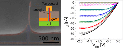
Vertical junctionless transistors with a gate-all-around (GAA) structure based on Ge/Si core/shell nanowires epitaxially grown and integrated on a ⟨111⟩ Si substrate were fabricated and analyzed. Because of efficient gate coupling in the nanowire-GAA transistor structure and the high density one-dimensional hole gas formed in the Ge nanowire core, excellent P-type transistor behaviors with Ion of 750 μA/μm were obtained at a moderate gate length of 544 nm with minimal short-channel effects. The experimental data can be quantitatively modeled by a GAA junctionless transistor model with few fitting parameters, suggesting the nanowire transistors can be fabricated reliably without introducing additional factors that can degrade device performance. Devices with different gate lengths were readily obtained by tuning the thickness of an etching mask film. Analysis of the histogram of different devices yielded a single dominate peak in device parameter distribution, indicating excellent uniformity and high confidence of single nanowire operation. Using two vertical nanowire junctionless transistors, a PMOS-logic inverter with near rail-to-rail output voltage was demonstrated, and device matching in the logic can be conveniently obtained by controlling the number of nanowires employed in different devices rather than modifying device geometry. These studies show that junctionless transistors based on vertical Ge/Si core/shell nanowires can be fabricated in a controlled fashion with excellent performance and may be used in future hybrid, high-performance circuits where bottom-up grown nanowire devices with different functionalities can be directly integrated with an existing Si platform.
中文翻译:

垂直Ge / Si核/壳纳米线无结晶体管
制作并分析了基于外延生长并集成在⟨111⟩Si衬底上的Ge / Si核/壳纳米线的具有全栅(GAA)结构的垂直无结晶体管。由于纳米线-GAA晶体管结构中的有效栅极耦合以及Ge纳米线核心中形成的高密度一维空穴气体,I导通时具有出色的P型晶体管性能。在544 nm的中等栅极长度下获得750μA/μm的光,最小的短沟道效应。可以通过具有很少拟合参数的GAA无结晶体管模型对实验数据进行定量建模,这表明可以可靠地制造纳米线晶体管,而无需引入会降低器件性能的其他因素。通过调节蚀刻掩模膜的厚度,可以容易地获得具有不同栅极长度的器件。对不同器件的直方图进行分析,得出器件参数分布中有一个主要的峰,这表明出色的均匀性和单纳米线操作的高置信度。通过使用两个垂直纳米线无结晶体管,演示了具有接近轨到轨输出电压的PMOS逻辑逆变器,通过控制不同设备中采用的纳米线的数量而不是修改设备的几何形状,可以方便地获得与逻辑上的设备匹配。这些研究表明,基于垂直Ge / Si核/壳纳米线的无结晶体管可以以可控的方式制造,并具有出色的性能,并且可以用于未来的混合,高性能电路中,其中可以自底向上生长具有不同功能的纳米线器件。与现有的Si平台直接集成。
更新日期:2015-12-21
中文翻译:
垂直Ge / Si核/壳纳米线无结晶体管
制作并分析了基于外延生长并集成在⟨111⟩Si衬底上的Ge / Si核/壳纳米线的具有全栅(GAA)结构的垂直无结晶体管。由于纳米线-GAA晶体管结构中的有效栅极耦合以及Ge纳米线核心中形成的高密度一维空穴气体,I导通时具有出色的P型晶体管性能。在544 nm的中等栅极长度下获得750μA/μm的光,最小的短沟道效应。可以通过具有很少拟合参数的GAA无结晶体管模型对实验数据进行定量建模,这表明可以可靠地制造纳米线晶体管,而无需引入会降低器件性能的其他因素。通过调节蚀刻掩模膜的厚度,可以容易地获得具有不同栅极长度的器件。对不同器件的直方图进行分析,得出器件参数分布中有一个主要的峰,这表明出色的均匀性和单纳米线操作的高置信度。通过使用两个垂直纳米线无结晶体管,演示了具有接近轨到轨输出电压的PMOS逻辑逆变器,通过控制不同设备中采用的纳米线的数量而不是修改设备的几何形状,可以方便地获得与逻辑上的设备匹配。这些研究表明,基于垂直Ge / Si核/壳纳米线的无结晶体管可以以可控的方式制造,并具有出色的性能,并且可以用于未来的混合,高性能电路中,其中可以自底向上生长具有不同功能的纳米线器件。与现有的Si平台直接集成。


 京公网安备 11010802027423号