Nano-Micro Letters ( IF 31.6 ) Pub Date : 2017-02-14 , DOI: 10.1007/s40820-017-0132-x Dainan Zhang , Tianlong Wen , Ying Xiong , Donghong Qiu , Qiye Wen
|
Abstract
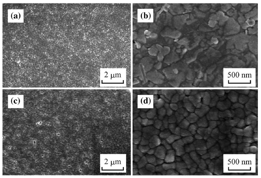
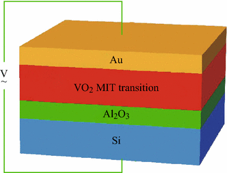
VO2 thin films were grown on silicon substrates using Al2O3 thin films as the buffer layers. Compared with direct deposition on silicon, VO2 thin films deposited on Al2O3 buffer layers experience a significant improvement in their microstructures and physical properties. By optimizing the growth conditions, the resistance of VO2 thin films can change by four orders of magnitude with a reduced thermal hysteresis of 4 °C at the phase transition temperature. The electrically driven phase transformation was measured in Pt/Si/Al2O3/VO2/Au heterostructures. The introduction of a buffer layer reduces the leakage current and Joule heating during electrically driven phase transitions. The C–V measurement result indicates that the phase transformation of VO2 thin films can be induced by an electrical field.
中文翻译:

铝的影响
摘要
使用Al 2 O 3薄膜作为缓冲层,在硅衬底上生长VO 2薄膜。与直接沉积在硅上相比,沉积在Al 2 O 3缓冲层上的VO 2薄膜的微观结构和物理性能有了显着改善。通过优化生长条件,VO 2薄膜的电阻可以改变四个数量级,同时在相变温度下的热滞回落降低为4°C。在Pt / Si / Al 2 O 3 / VO 2中测量了电驱动的相变/ Au异质结构。缓冲层的引入减少了电驱动相变期间的泄漏电流和焦耳热。所述Ç - V测量结果表明,VO的相变2薄膜可以通过电场来诱导。











 京公网安备 11010802027423号